TRANSISTORS
Bipolar Junction Transistors (BJTs)
| Date Published: | |
| Last Modified: |
Overview
Bipolar junction transistors (BJTs) are 3 legged active semiconductor devices. They behave as a current-amplifier, amplifying a small base-emitter (BE) current into a larger collector-emitter (CE) current.
It was the first type of transistor to ever be mass produced.
Types
BJTs come in two flavours, NPN or PNP. They both have three terminals, the collector ©, the base (B) and the emitter (E).
The differences between the NPN and PNP transistor types are analogous to the N-Channel and P-Channel MOSFET types.
Schematic Symbols
The schematic symbols for NPN and PNP transistors are shown below:

Schematics symbols for NPN and PNP transistors. Note that the collector and emitter have flipped positions for the PNP, as commonly drawn on schematics.
Notice that the collector and emitter have been flipped for the PNP (compared to the NPN), this is how they are normally drawn on schematics.
The arrow is always on the emitter leg of the BJT. To differentiate between the two, the arrow on the NPN points away from the transistor, the arrow on a PNP points towards the transistor.
Sometimes you will see the transistors drawn with circles around them, they represent exactly the same thing as the symbols above.
How They Work
BJTs are made from a hunk of silicon. They are either a thin slice of P-type semiconductor sandwiched between two layers of N-type semiconductor (NPN) or the reverse, a thin slice of N-type semiconductor sandwiched between two layers of P-type semiconductor (PNP).
The bipolar part of their name comes from the fact they conduct by using both majority and minority charge carriers.
Important Parameters
Gain (hfe)
The gain of a BJT is the ratio between the base current and the collector current.
Circuit Design Basics With BJTs
The current through the base pin (\(I_b\)) and the current through the collector pin (\(I_c\)) always sums to give the current through the emitter pin (\(I_e\)).
Because the collector current is usually much larger than the base current, for most scenarios you can treat the collector and emitter current as equal.
As a general rule, NPN transistors are useful for connecting things to ground. PNP transistors are useful for connecting things to your power rail.
NPNs require a small positive base-emitter voltage to create a current which flows into the base. This current, multiplied by the gain of the transistor, determines the collector-to-emitter current (well, to be technically correct, the maximum collector current). Because of this, a NPN transistor will only conduct when both the base and collector have a higher voltage than the emitter.
A PNP transistor will only conduct when both the base and collector have a negative voltage w.r.t the emitter.
High And Low-side Switching With BJTs
NPN transistors are good for low-side switching. You can connect the collector to the negative end of the load, the emitter to ground, and control the base with a digital low/high signal through a resistor (low/ground base signal = load off, high base signal = load on).
They are not so good for high-side switching, as negative feedback prevents them from entering saturation. Normally you would want to use a PNP transistor. However, in some situations, using a NPN transistor for high-side switching can be advantageous. This configuration is also called a common collector amplifier.
PNP transistors are good for high-side switching. Although not great at low-side switching, they can be used in some cases.
Amplifier Topologies
Common Collector
The common collector amplifier topology is also known as a emitter follower amplifier.

The output voltage is almost equal to the input voltage, except for an approximately 0.7V diode drop. This means that the amplifier has a voltage gain of almost unity (1), or \(0dB\).
Here is a graph of \(v_{in}\) vs. \(v_{out}\) for the above circuit:

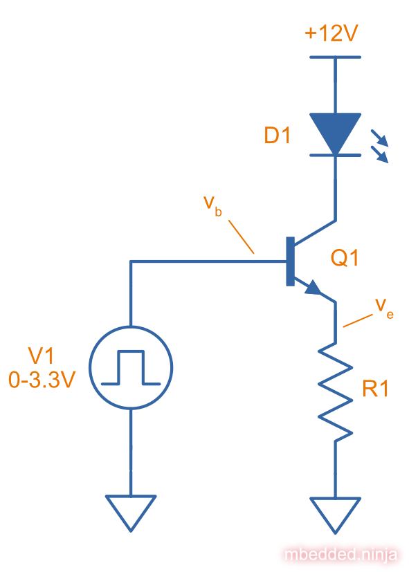
Constant-Current Sink
BJTs can be configured to sink a relatively constant amount of current which is independent on the output-side voltage. This can be a useful way of driving an LED from a microcontroller with a constant current, no matter what voltage source is used to drive the LED.

The above schematic was designed to drive the LED with 10mA of current when the BJT was driven from a microcontroller running at +3.3V. Since +3.3V is applied to the base of the NPN transistor, the transistor will always turn on just enough so that the voltage at the emitter is 0.7V less, e.g.
Since we know the emitter voltage is going to be +2.6V, we can choose the right resistor, \(R_1\) to get the LED current we desire (remember that the current out of the emitter is pretty much equal to the current into the collector).
So if we want a LED current of 10mA, that means we need \(R1 = 260\Omega\). The closest E12 value is \(270\Omega\).
Notice how the LED current is independent of the +12V. The +12V can change to say, +9V and the LED current will still be 10mA. The current draw from the microcontroller into the base of the transistor will be very low (somewhere around 100uA).
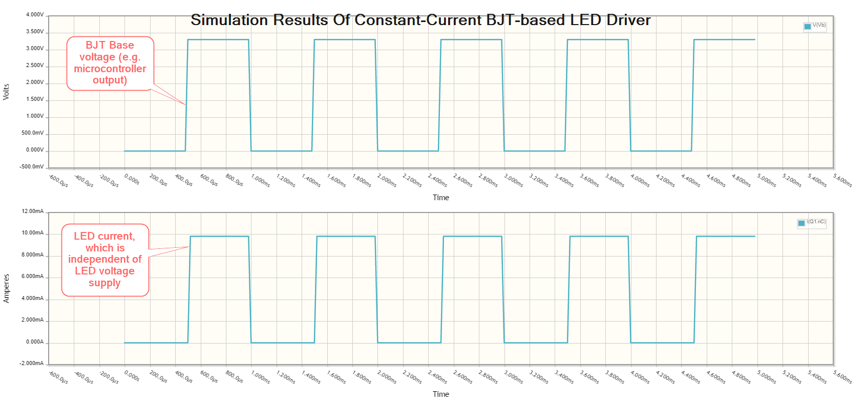
Below are the simulation results for the above schematic, showing the LED current to be indeed 10mA. It works!

Common BJTs
548 and 558 are common numbers to see embedded in transistor part numbers.
BC548 - Common NPN transistor
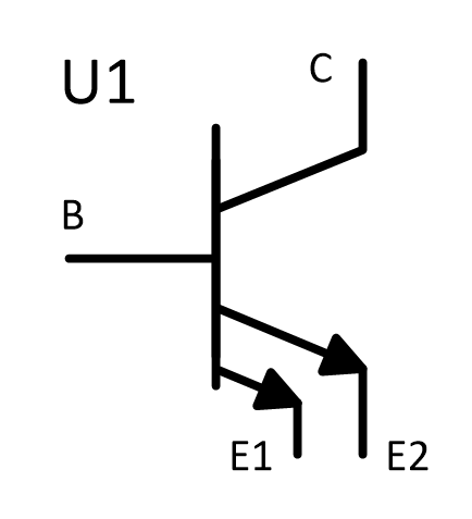
Multiple-Collector And Multiple-Emitter BJTs
Multiple emitter and multiple collector BJTs are special types of BJTs which have more than one emitter or more than one collector.

In the case of a multiple collector BJT, the total collector current \(I_{C,tot}\) is set by the base current \(I_B\). If all the collectors are the same size (the silicon is physically the same size), then the current is equally split across all collectors.
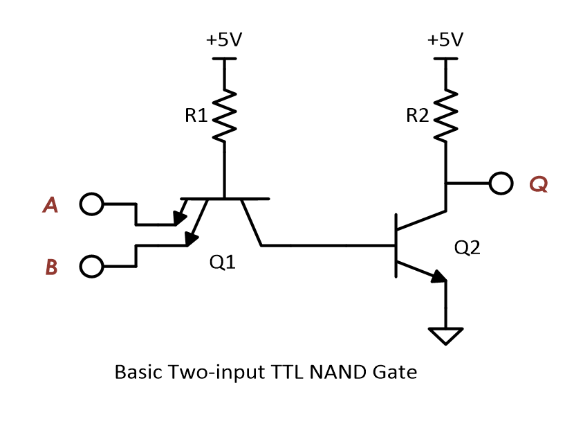
The multiple-emitter BJT can be used to implement AND logic. The multiple-emitter BJT forms an integral part of the TTL AND input circuitry (e.g. the 7400 series of integrated circuits). They were introduced into digital logic design to replace the diodes of diode-transistor logic (DTL), with the advantage of a lower switching time and lower power dissipation.

Multiple emitter BJTs were also used in older (e.g. from the 1960’s) RAM. For example, Intel’s first IC, the 3101 (64 bits of RAM!), contains multiple emitter BJTs as part of the 2-state latch circuitry which holds one bit of information. One emitter is used to select which cell to read or write, while the other emitter is used to read or write the data. See an excellent tear-down of the IC on Ken Shirriff’s blog.
External References
This is a great video on two not-so-common transistor biasing configurations.